Multilayer Solder Mask Blind Buried Via PCB Prototype Service Gold Finger
CESGATE's products are widely used in mobile phones, computers, automobiles, communication equipment, servers, industrial control and other electronic information fields. Adhering to the focus on the pressure and challenges of customers in the field of electronic information, to provide customers with competitive circuit boards and services, and continue to create maximum value for customers. Adhere to customer achievement, hard work, open innovation, self-criticism. CESGATE will grow into the world's leading circuit board manufacturer.
From the perspective of the industrial chain, the upstream of the printed circuit board industry chain is the raw material supplier, including copper foil, ink, resin, glass fiber cloth and other raw materials, of which copper foil and glass fiber cloth are the main raw materials for printed circuit boards; the midstream is the printed circuit board. The production layer of the board, the multi-layer board is the product with the largest output value in the printed circuit board in my country, accounting for more than 45.8%; the downstream is the application layer, and the printed circuit board has a wide range of applications, involving communications, automotive electronics, consumer Electronics, aerospace, medical equipment and other fields.
What is a Printed Circuit Board (PCB)
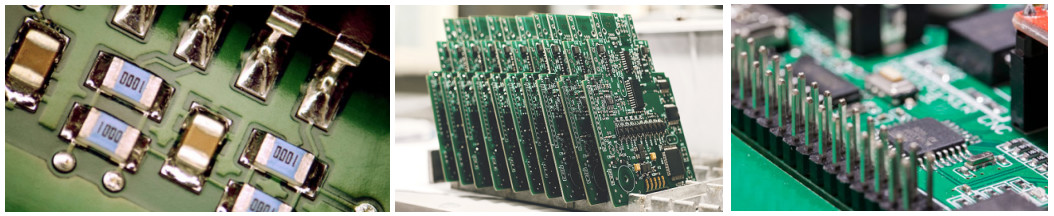
Printed circuit board, also known as printed circuit board, printed circuit board, often used in English abbreviations are PCB (Printed circuit board) or PWB (Printed wire board). PCB is the base plate used to assemble electronic components, and it is also the "mother of electronic products". It is a very important electronic component and a support for electronic components. Mainly through the metal copper foil circuits on the board, through the design of each layer to connect and conduct related components, to achieve a complete product that operates effectively.
Before the early PCB appeared, the various components of electronic products were connected by wires to form a complete path. Later, in order to simplify the manufacturing process of electronic products and reduce the cost, the circuit was developed by printing, and the copper foil on the substrate was used to replace the original wire connection, thereby improving the production efficiency.
The various components are mainly connected through the metal copper foil circuits on the board. By designing each layer to connect and conduct related components, a complete product that operates effectively is achieved.
The traditional circuit board construction method uses printed resists to make circuit lines and drawings, so it is called printed circuit board. Because the size of electronic products continues to be miniaturized and refined, most circuit boards are currently covered with etching resists (wet film or dry film), which are exposed and developed and then etched to remove unwanted copper foil to make circuit boards.
PCB Prototype Service Capacities and Technical Specification
| NO. | Items | Capabilities |
| 1 | Layers | 2-68L |
| 2 | Maximum machining size | 600mm*1200mm |
| 3 | Board thickness | 0.2mm-6.5mm |
| 4 | Copper thickness | 0.5oz-28oz |
| 5 | Min trace/space | 2.0mil/2.0mil |
| 6 | Minimum finished aperture | 0. 10mm |
| 7 | Maximum thickness to diameter ratio | 15:1 |
| 8 | Via treatment | Via, blind&buried via, via in pad, Copper in via … |
| 9 | Surface finish/treatment | HASL/HASL lead free, Chemical tin, Chemical Gold, Immersion gold Inmersion Silver/Gold, Osp, Gold Plating |
| 10 | Base Material | FR408 FR408HR, PCL-370HR;IT180A, Megtron 6(Panasonic);Rogers4350,
Rogers4003, RO3003, Rogers/Taconic/Arlon/Nelco laminate with FR-4 material(including partial Ro4350B hybrid laminating with FR-4) |
| 11 | Solder mask color | Green.Black.Red.Yellow.White.Blue.Purple.Matte Green. Matte Black |
| 12 | Testing Service | AOI, X-Ray, Flying-Probe, Function Test, First Article Tester |
| 13 | Profiling Punching | Routing,V-CUT,Beveling |
| 14 | Bow&twist | ≤0.5% |
| 15 | HDI type | 1+n+1,2+n+2,3+n+3 |
| 16 | Min mechanical aperture | 0.1mm |
| 17 | Min laser aperture | 0.075mm |
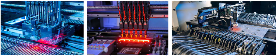
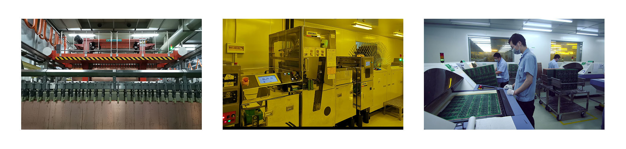
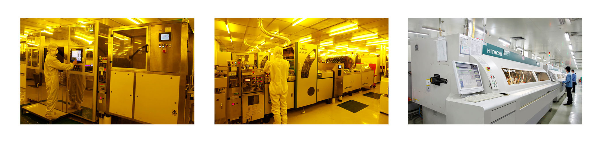
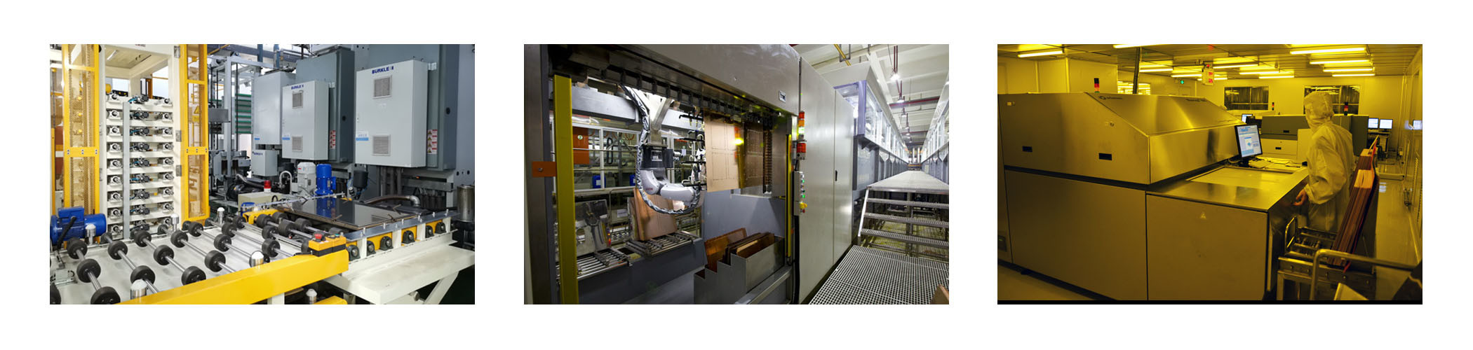
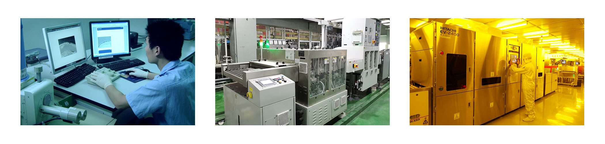
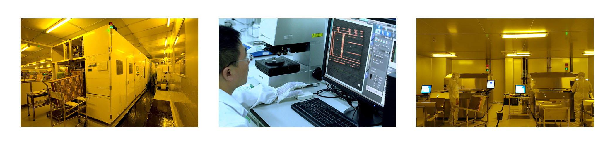
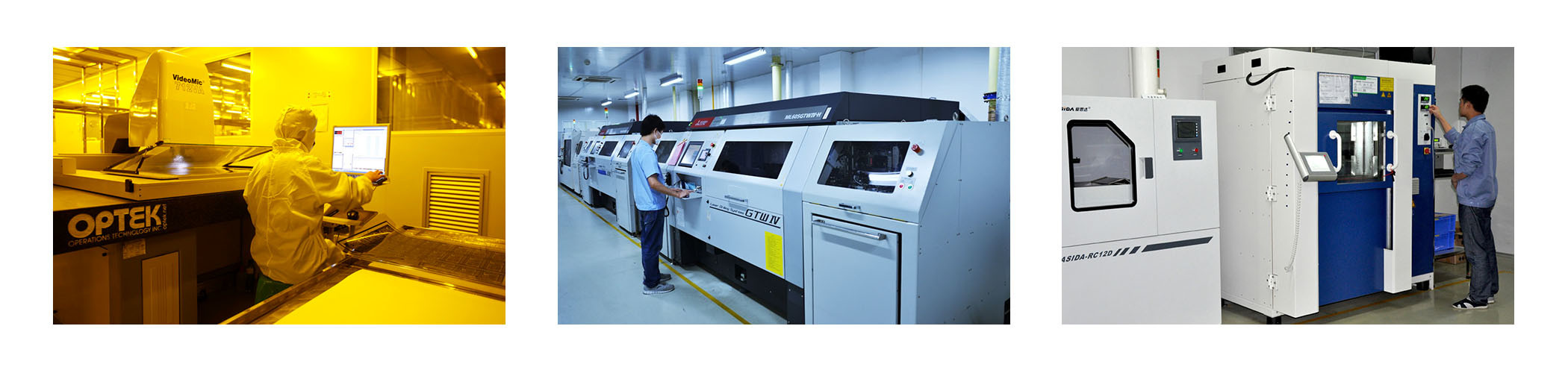
Chengdu Cesgate Technology Co., Ltd. is located in Chengdu High-tech Zone, Sichuan, China, with a standardized modern industrial plant of about 4,000 square meters. The company is a leading electronic manufacturing service provider in Chengdu. The factory has passed the ISO9001 quality management system certification and ISO14001 environmental protection system certification issued by SGS. Since its establishment, the company has adhered to the business philosophy of "professional quality, continuous innovation, and high-quality service".

FAQ
Q.Shipping cost?
CESGATE: The shipping cost is determined by the destination, weight, packing size of the goods. Please let us know if you need us to quote you the shipping cost. |
Q: What certificates do you have?
CESGATE: We have ISO 9001, ISO14001 and UL certificates. |
Q: Which express companies do you cooperate with?
CESGATE: We cooperate with express companies, including DHL, FedEX, UPS, TNT and EMS. And we also have our own freight forwarders, with lower shipping fees. |
Q: What modes of transport are there?
CESGATE: Usually includes express, air shipment, rail shipment and sea shipment. |
Q: Popular field?
CESGATE: Semiconductor, Smart Home, Medical Products, Smart Wearable, Industrial Control, IOT etc. |
Q: Can you give us a preferential discount?
CESGATE: Of course, we will offer a preferential discount for your large orders and confirm the order quickly. |
Product Tags:

|
|
Multilayer Solder Mask Blind Buried Via PCB Prototype Service Gold Finger Images
|