Quick Turn Rigid PCB Prototype Service Surface Treatment Blind&Buried Hole
Technical Requirement for PCB assembly service:
1) Professional Surface-mounting and Through-hole soldering Technology
2) Various sizes like 1206, 0805, 0603 components SMT technology
3) ICT(In Circuit Test),FCT(Functional Circuit Test) technology.
4) PCB assembly service With CE, FCC, Rohs Approval
5) Nitrogen gas reflow soldering technology for SMT.
6) High Standard SMT&Solder Assembly Line
7) High density interconnected board placement technology capacity.

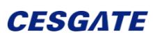
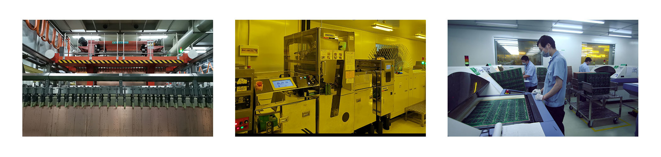
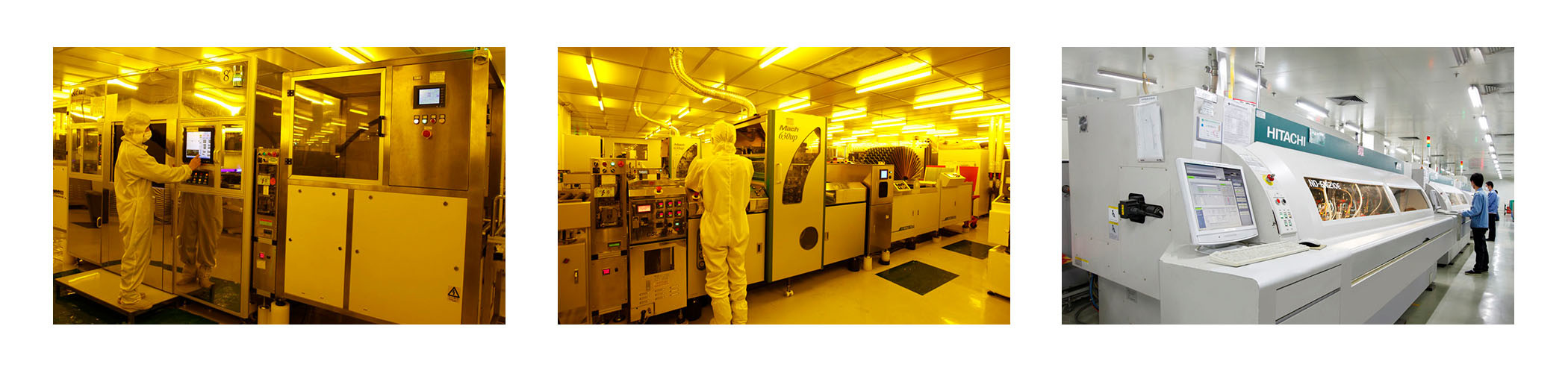
Copper patterning
In PCB assembly service,The first step is to replicate the pattern in the fabricator's CAM system on a protective mask on the copper foil PCB layers. Subsequent etching removes the unwanted copper unprotected by the mask. (Alternatively, a conductive ink can be ink-jetted on a blank (non-conductive) board. This technique is also used in the manufacture of hybrid circuits.)
- Silk screen printing uses etch-resistant inks to create the protective mask.
- Photoengraving uses a photomask and developer to selectively remove a UV-sensitive photoresist coating and thus create a photoresist mask that will protect the copper below it. Direct imaging techniques are sometimes used for high-resolution requirements. Experiments have been made with thermal resist. A laser may be used instead of a photomask. This is known as maskless lithography or direct imaging.
- PCB milling uses a two or three-axis mechanical milling system to mill away the copper foil from the substrate. A PCB milling machine (referred to as a 'PCB Prototyper') operates in a similar way to a plotter, receiving commands from the host software that control the position of the milling head in the x, y, and (if relevant) z axis.
- Laser resist ablation Spray black paint onto copper clad laminate, place into CNC laser plotter. The laser raster-scans the PCB and ablates (vaporizes) the paint where no resist is wanted. (Note: laser copper ablation is rarely used and is considered experimental.
- Laser etching The copper may be removed directly by a CNC laser. Like PCB milling above this is used mainly for prototyping.
- EDM etching uses an electrical discharge to remove a metal from a substrate submerged into a dielectric fluid
The method chosen depends on the number of boards to be produced and the required resolution.
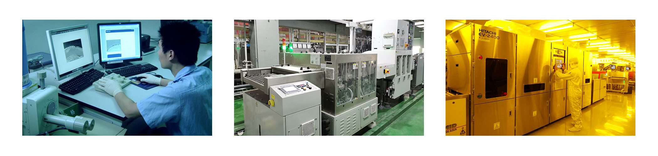
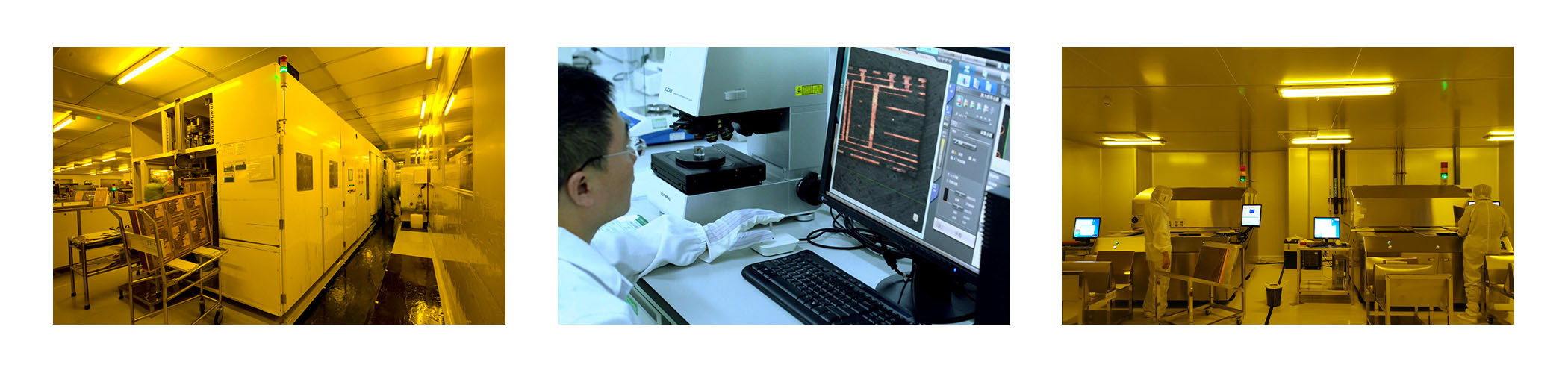
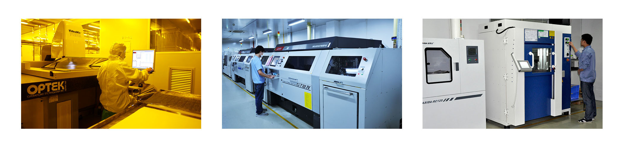
PCB Prototype Service Capacities and Technical Specification
| NO. | Items | Capabilities |
| 1 | Layers | 2-68L |
| 2 | Maximum machining size | 600mm*1200mm |
| 3 | Board thickness | 0.2mm-6.5mm |
| 4 | Copper thickness | 0.5oz-28oz |
| 5 | Min trace/space | 2.0mil/2.0mil |
| 6 | Minimum finished aperture | 0. 10mm |
| 7 | Maximum thickness to diameter ratio | 15:1 |
| 8 | Via treatment | Via, blind&buried via, via in pad, Copper in via … |
| 9 | Surface finish/treatment | HASL/HASL lead free, Chemical tin, Chemical Gold, Immersion gold Inmersion Silver/Gold, Osp, Gold Plating |
| 10 | Base Material | FR408 FR408HR, PCL-370HR;IT180A, Megtron 6(Panasonic);Rogers4350,
Rogers4003, RO3003, Rogers/Taconic/Arlon/Nelco laminate with FR-4 material(including partial Ro4350B hybrid laminating with FR-4) |
| 11 | Solder mask color | Green.Black.Red.Yellow.White.Blue.Purple.Matte Green. Matte Black |
| 12 | Testing Service | AOI, X-Ray, Flying-Probe, Function Test, First Article Tester |
| 13 | Profiling Punching | Routing,V-CUT,Beveling |
| 14 | Bow&twist | ≤0.5% |
| 15 | HDI type | 1+n+1,2+n+2,3+n+3 |
| 16 | Min mechanical aperture | 0.1mm |
| 17 | Min laser aperture | 0.075mm |
Why choose CESGATE?
CESGATE is a team with more than 10 years experience in the field. We owns abundant experiences for serving overseas customers from industrial automatic control, communication, medical, Auto and consumer electronics,etc. We test our product strictly to guarantee the quality to our customers. We accumulate high reputation during our cooperation.You will achieve following value-added services when you cooperate with us:
One-stop PCB/PCBA Service
Optimizing your PCB design during production
Satisfied quality with competitive prices
Instant response in both quotation and delivery
Increase your business with our powerful support

FAQ
Q: Why should we buy from CESGATE?
CESGATE: Professional and experienced R&D team. Advanced production equipment, scientific and reasonable process flow.
Reliable and strict quality control system. We test all our products before shipment to make sure everything is in perfect condition. From the design to the complete product, CESGATE's professional team will put you at ease |
Q: How long is the shelf life of the PCB board and how should it be stored?
CESGATE: 25℃ / 60%RH is recommended when the PCB is stored. The plate itself has no shelf life, but if it exceeds three months, it needs to be baked to remove moisture and stress, and it should be used immediately after baking. It is recommended that the pieces should be loaded within 6 months of storage to reduce the phenomenon of rejection and explosion. |
Q: Can we inspect quality during production?
CESGATE: Yes, we are open and transparent on each production process with nothing to hide. We welcome customer inspect our production process and check in house. |
Q: What are the main products of your PCB/PCBA services?
CESGATE: Our PCB/PCBA services are mainly for the industries including Medical, Automotive, Energy, Metering/Measurements, Consumer Electronics. |
Q: What are the common substrates of CESGATE?
A:Tg-140: ISOLA FR402 / NAN-YA NP-140
Tg-150: ISOLA IS400 / NAN-YA NP-155
Tg-170~180: ISOLA 370HR / NPN-YA / NAN-YA NP-175F |
Product Tags:

|
|
Quick Turn rigid PCB Prototype Service Surface Treatment Blind&Buried Hole Images
|